Quantcast
Channel: Sound - Audio Projects - PIC Microcontroller
Viewing all 110 articles
Browse latest View live

MIDI Chord Button Keyboard Using PIC18F4620 part 3

$
0
0

Connections
The following table documents the connecting leads and molex pin-header numbers tying the various interfaces together.

Header Pin no. Signal/Function Direction Header Pin no. Signal/Function
Chord Controller-SV1 1 RD7 ——> Matrix Decoder-SV4 1 Chord Sel. C
Chord Controller-SV1 2 RD6 ——> Matrix Decoder-SV4 2 Chord Sel. B
Chord Controller-SV1 3 RD5 ——> Matrix Decoder-SV4 3 Chord Sel. A
Chord Controller-SV1 4 RD4 ——> Matrix Decoder-SV4 4 Note Sel. E
Chord Controller-SV2 1 RD3 ——> Matrix Decoder-SV1 1 Note Sel. D
Chord Controller-SV2 2 RD2 ——> Matrix Decoder-SV1 2 Note Sel. C
Chord Controller-SV2 3 RD1 ——> Matrix Decoder-SV1 3 Note Sel. B
Chord Controller-SV2 4 RD0 ——> Matrix Decoder-SV1 4 Note Sel. A
Chord Controller-SV4 1 +5v ——> Matrix Decoder-SV7 1 +5v
Chord Controller-SV4 2 N/C Matrix Decoder-SV7 3 W (KEYDOWN)
Chord Controller-SV4 3 RB1 <—— Matrix Decoder-SV7 2 Y (/KEYDOWN)
Chord Controller-SV4 4 GND ——> Matrix Decoder-SV7 4 GND
Chord Controller-SV3 1 RC2 <—— Keypad-X1 6 In S3, 7, 11, 15
Chord Controller-SV3 2 RC1 <—— Keypad-X1 7 In S2, 6, 10, 14
Chord Controller-SV3 3 RC0 <—— Keypad-X1 8 In S1, 5, 9, 13
Chord Controller-SV3 4 RE2 <—— Keypad-X1 5 In S4, 8, 12, 16
Chord Controller-SV8 3 RB4 ——> Keypad-X1 1 Out S13-S16
Chord Controller-SV8 4 RB5 ——> Keypad-X1 2 Out S9-S12
Chord Controller-SV8 5 RB6 ——> Keypad-X1 3 Out S5-S8
Chord Controller-SV8 6 RB7 ——> Keypad-X1 4 Out S1-S4
Chord Controller-X3 1 /MCLR <—— Keypad-X2 1 RESET
Chord Controller-SV6 1 RC3 ——> Keypad-X2 2 LED1
Chord Controller-SV6 2 RC4 ——> Keypad-X2 3 LED2
Chord Controller-SV6 3 RC5 ——> Keypad-X2 4 LED3
Chord Controller-SV6 4 GND ——> Keypad-X2 5 GND
Chord Controller-SV6 5 +5v ——> Keypad-X2 6 +5v
Chord Controller-SV9 1 TX/RC6 (via 220R) ——> DIN SOCKET 5 MIDI-OUT
Chord Controller-SV9 2 GND ——> DIN SOCKET SCR Screen
Chord Controller-SV9 3 +5v (via 220R) ——> DIN SOCKET 4 MIDI-OUT
Chord Controller-SV10 1 +5v ——> Volume Pot LH Tag Top
Chord Controller-SV10 2 AN5 <—— Volume Pot Middle Tag Slider
Chord Controller-SV10 3 GND ——> Volume Pot RH Tag GND
Chord Controller-SV11 1 +5v ——> Pitch-wheel Pot LH Tag Top
Chord Controller-SV11 2 AN6 <—— Pitch-wheel Pot Middle Tag Slider
Chord Controller-SV11 3 GND ——> Pitch-wheel Pot RH Tag GND
Chord Controller-SV7 1 GND ——> FTDI-USB RS232-TTL 1 GND
Chord Controller-SV7 4 RX/RC7 <—— FTDI-USB RS232-TTL 4 (PC) TX
Chord Controller-SV7 5 TX/RC6 ——> FTDI-USB RS232-TTL 5 (PC) RX

Other connectors are documented on the schematic.
Note that I used a 10K Lin pot for the pitch wheel and 10K log for the volume pot. Although these values are a little on the high side for efficient analog conversion, in practise they work fine.

Chord Button Keyboard Shift Bar

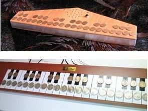
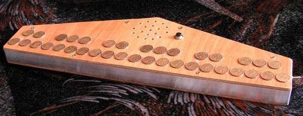
I had originally intended to build the key matrix on a printed circuit board, and this would still be the preferred solution. Two thing deterred me. First, placement of the 6X6mm TACT switches on the PCB using the default outlines supplied in Eagle would have meant a longer keyboard than I wanted, and secondly, My Eagle license only allows Eurocard size boards – meaning there would be 3 boards to join together for the matrix. These two factors represented enough reason to look for another solution. I finally plumped for a single longish piece of matrix board. This allowed the key matrix to have the desired spacing – I fore-shortened the distance between each tag on the switches to 0.2 inches by straightening these close to the body of the switch, which then allowed a switch-to-switch pitch of 0.6 inches.
In solving one problem however, I created another. Mounting the finished board proved fiddly and difficult, and a solution using nylon nuts and bolts had to be adopted – you have been warned!
I terminated the matrix with 2 IDC headers – one 10-way and the other 20-way. Because my finished matrix was hand-wired, I haven’t given connection details for this, and you should refer to the matrix decoder schematic for connection details.
I’ve included a suggested matrix schematic in with the main Eagle project files, should you wish to augment this. A snapshot of this is given below:

Chord Shift Switch
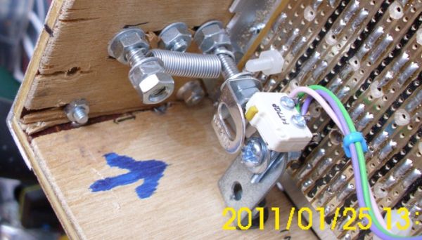
I made provision for plugging in a foot-switch, but as the floor in front of me is rather busy when I’m playing, also provided a handy switch bar on the unit. It is crude but effective, and I’ll briefly describe it here.
A piece of 4mm (0.196 inch) diameter bright drawn mild steel was bent at 90deg each end so to form a bar 305mm (12 inch) long, with two short arms projecting roughly 40mm (~1.5inch) and 50mm. (2 inch) A thread was cut on each arm (I used M4), so that when the bar is placed through two locating holes on the front of the keyboard cabinet, and a washer and nut are threaded onto each arm, the shift bar is approximately 20mm from the keyboard cabinet front. (0.75inch)
Two small metal plates (I used Meccano) are fixed over the two holes on the cabinet front, and 2 collets (4mm) are fixed on each of the shift bar’s arms, which are then pushed into place in the cabinet.


For more detail: MIDI Chord Button Keyboard Using PIC18F4620 part 3

Current Project / Post can also be found using:

  • free sound echo circuit project pdf
  • which pic microcontroller is best for the interface of cmvoice synthesiser and play back

The post MIDI Chord Button Keyboard Using PIC18F4620 part 3 appeared first on PIC Microcontroller.


Treslie – A 3-phase speaker system for Leslie emulation using PIC18F26K20

$
0
0

This post describes the design and construction of a 3-phase loudspeaker intended for Leslie Speaker emulation. The unit is intended to be driven by a 3-channel audio amplifier The Brute, which in turn is controlled by LEMS, a micro-controller based control system, the construction of which both are described in companion posts.

3-phase speaker system

Companion posts are as follows:

Why Treslie?

Well, I once knew a girl with three heads.. No, you wouldn’t swallow that. But the name I’ve adopted is apparently quite common in the USA as a girl’s name. In fact it isn’t hard and you’ve probably already guessed that’s it’s a conflation of tres – meaning 3 (in spanish etc.) , and lie, the last part of Leslie. Whimsy? Probably, but I needed to call it something.

I’ve lifted a small part of text from the LEMS post which I hope clarifies what is being attempted, and this is given below:

I made the long sides ~12 inches (300mm), and the short sides ~6 inches (150mm). This gives an external angle of 120 degrees between the polar plane of each loudspeaker chassis. With an external height (on my cabinets) of around 27.5 inches (698mm), this gives a total volume of around 2.5 cu ft. Internal volume will be a little less than this, and of course each loudspeaker has only 1/3 of the volume, because of the 3 central partitions.

Each compartment should be made as airtight as possible – mainly due to the use of high-compliance (long-throw) loudspeaker units. These give good bass response in small cabinets, but require near-sealed enclosures, if damaging over-excursion of the loudspeaker cone is to be avoided. I found that screwed joints and the liberal use of a bathroom sealant that remains plastic when dry is the best solution. I advise against the use of glue. Access for maintenance would necessitate damaging a glued cabinet. With the sealant used, panels are easily disassembled, and the sealant can be simply replaced.

As this unit was intended to be experimental, and for use mainly at home with a small 70’s organ, and my guitars, I decided to cater for no more than about 30watts per channel, this keeps costs and size down, and allowed for the purchase of 3 reasonably-priced high-compliance units from my local stockist.
The loudspeakers are complimented with 3 cheap piezo horn units. Information on these suggested the use of series connected 47ohm resistors – I ignored this for the input powers I was using, and connected these up without the series resistor, to no ill effect.

Despite the loudspeaker units being cheap, it is worthwhile incorporating a suitable fuse in series. I used a 20mm, 1.6amp quick-blow item, that will protect the loudspeaker against gross DC flow. Too many loudspeaker designs omit this simple protection, with dire results in the case of accidents. The screw-in fuse-holders were sited on a small panel alongside the loudspeaker 4mm connector sockets.

Materials.
The sides were all made from reclaimed chipboard, mostly melamine-covered, of the type used for kitchen cabinet carcasses and cheap 70’s fitted wardrobes. The top and bottom were made from .. .. new chipboard, and the loudspeaker grilles from … new MDF.

Internal bracing was all new wood – mostly offcuts and scraps 3/4 X 3/4 inch (20mm X 20mm).

The sound absorbent material filling each speaker compartment has one important criteria – it should contain bubbles. Bubbles are just great at absorbing (converting to heat) the sound energy that would otherwise bounce around the hard reflective inner surfaces of the cabinet. Don’t let merchants sell you grossly over-priced ‘wadding’. My experiments have shown good results with: a) The remains of old hollow-fill pillows or cushions; b) Bubble-wrap; and c) Expanded polystyrene. All of these can be hoarded until needed – the latter two are usually used as packing materials for stuff delivered to your door.


For more detail: Treslie – A 3-phase speaker system for Leslie emulation using PIC18F26K20

Current Project / Post can also be found using:

  • pic16f877 5 1 audio system
  • dspic audio midi
  • ic pic sound effect
  • microcontroller audio project

The post Treslie – A 3-phase speaker system for Leslie emulation using PIC18F26K20 appeared first on PIC Microcontroller.

Wave audio player using PIC16F887 microcontroller

$
0
0

This small project shows how to make a simple wave audio player using PIC16F887 microcontroller and SD card. The WAV audio file used in this project is 8000 Hz, 8-bit stereo (2 channels).
Hardware Required:

Wave audio player using PIC16F887 microcontroller

  • PIC16F887 microcontroller
  • SD card (formatted with FAT16 or FAT32 file system)
  • ASM1117 3.3 voltage regulator
  • Audio amplifier (ex: PC speaker, LM386 ……)
  • Speaker
  • 20 MHz crystal oscillator
  • 2 x 22pF ceramic capacitors
  • 3 x 3.3K ohm resistor
  • 3 x 2.2K ohm resistor
  • 10K ohm resistor
  • 2 x 1K ohm resistor
  • 3 x 10uF polarized capacitor
  • 100nF ceramic capacitor
  • 5V Power source
  • Breadboard
  • Jumper wires

The Circuit:

The microcontroller generates audio using PWM technique, if the wave audio file is mono (1 channel) the microcontroller will generate only 1 PWM signal (PWM1) and hence we will hear the sound from 1 speaker only. If the wave audio file is stereo both speakers will give sound.
In this project the PIC16F887 runs with 20MHz crystal oscillator which is the maximum speed of this microcontroller, MCLR pin function is disabled.
The C code:
The C code below was tested with CCS C compiler versions 5.051.
In this project I used the FAT library (FAT16 and FAT32), its source file can be found in the the following topic:
SD card FAT library for CCS C compiler
I tested this project with FAT32 8 GB and FAT16 2 GB micro-SD cards.
The name of the wave audio file which I used was mywav (mywav.wav with the extension), its sample rate is 8000 Hz with 2 channels (stereo).

Wave audio player using PIC16F887 microcontroller schematics
First of all I initialized the SD card using the function: sdcard_init(); this function return 0 if the initialization was OK and non-zero if there was an error. After the initialization of the SD card I initialized the FAT file system using the function fat_init(); and then I opened the wave audio file with the pre-selected name mywav.wav, all the three previous function returns 0 if OK and no-zero if error.

Read more: Wave audio player using PIC16F887 microcontroller 

The post Wave audio player using PIC16F887 microcontroller appeared first on PIC Microcontroller.

Wave player using PIC18F4550 microcontroller

$
0
0

Making an audio player (.wav files) using PIC microcontroller is not complicated especially when the MCU has a PWM module. This topic shows how to build an audio player using PIC18F4550 microcontroller where the the file is stored in an SD card with FAT16 or FAT32 file system.
In this project I used a wave file with sample rate of 16000 Hz and 2 channels (stereo). The file I used originally it was an MP3 file and I converted it to 8-bit wav format using an audio converter named audacity, it is a free and open source audio software (site: http://www.audacityteam.org/).
Hardware Required:

Wave player using PIC18F4550 microcontroller

  • PIC18F4550 microcontroller
  • SD card
  • ASM1117 3.3 voltage regulator
  • Audio amplifier (ex: PC speaker, LM386 ……)
  • Speaker
  • 8 MHz crystal oscillator
  • 2 x 22pF ceramic capacitors
  • 3 x 3.3K ohm resistor
  • 3 x 2.2K ohm resistor
  • 10K ohm resistor
  • 1K ohm resistor
  • 2 x 10uF polarized capacitor
  • 100nF ceramic capacitor
  • 5V Power source
  • Breadboard
  • Jumper wires

Wave player using PIC18F4550 microcontroller schematics
The Circuit:

The AMS1117 3.3V voltage regulator is used to supply the SD card with 3.3V. Also 3 voltage dividers are used to step down the 5V which comes from the microcontroller (come from RD2, RC7 and RB1) to about 3V which is sufficient for the SD card. Each voltage divider consists of 2K2 and 3K3 resistors. Pin RB0 of the microcontroller is connected directly to the SD card MISO pin with a pull-up resistor of 10K ohm.
Hardware SPI module is used by the microcontroller to read data from the SD card, the SPI pins of the PIC18F4550 MCU are:

  • SD0 (RC7): connected to pin MOSI of the SD card
  • SCK (RB1): connected to pin SCK of the SD card
  • SDI (RB0): connected to pin MISO of the SD card

There is an other pin which is CS (Chip Select or slave select) can be connected to any digital output pin (defined in the code), this pin is connected to SS pin of the SD cards.

Wave player using PIC18F4550 microcontroller schematics
The audio is generated using PWM technique, basically the PIC18F4550 has two PWM modules and their output are RC2 and RC1 for PWM1 and PWM2 respectively. An audio amplifier is needed to amplify the audio. In my circuit I used PC speaker as an amplifier. If the audio is stereo (2 channels) connect the same amplification circuit and use PWM2 output pin (RC1).
In this project PIC18F4550 MCU runs with 8 MHz crystal oscillator and MCLR pin function is disabled.

Read more: Wave player using PIC18F4550 microcontroller 

The post Wave player using PIC18F4550 microcontroller appeared first on PIC Microcontroller.

ISD2560 VOICE RECORDING PLAYBACK PROJECT PIC16F84 CONTROLLED

$
0
0

ISD2560 to directly control the PIC16F84A, audio recordings and multiple block will be able to play. LSI can be driven directly speakers also, in view of the lack of volume, only added to the… Electronics Projects,ISD2560 Voice Recording Playback Project PIC16F84 Controlled “ccs c examples, microchip projects, microcontroller projects, pic16f84 projects, “

VOICE RECORDING PLAYBACK PROJECT

ISD2560 to directly control the PIC16F84A, audio recordings and multiple block will be able to play. LSI can be driven directly speakers also, in view of the lack of volume, only added to the amplifier IC. This volume 10 minutes to drive the speakers. One LSI chip for voice recording playback “ISD2560” using a simple audio recording and playback unit prototype it

ISD2560 is playing this voice recording, in the same basic configuration, the sampling frequency, Divided into the following series. The use of the series in the most wide-frequency band; Instead of recording time limited to 60 seconds.

PIC16F84 ISD2560 VOICE RECORDING PROJECT SCHEMATIC

VOICE RECORDING PROJECT SCHEMATICVOICE RECORDING PROJECT

The above configuration, PIC16F84 controlled CCS C program written in C language ISD2560 directly as a result. LSI around as a standard configuration, so as MDS. Address the problem of how to control, but trying to control all the bits and 10 bits will be necessary in the event. Therefore, a control unit 64 and the lower six bits is 0 and leave it. This control is not only necessary to address the 4-bit, and easy configuration. Eventually 6.4 × 19 seconds blocks can be controlled. From the PIC, as well as switch addresses can be specified in order to make it possible to switch. The switch is using 4-bit DIP switch.

Source: ISD2560 VOICE RECORDING PLAYBACK PROJECT PIC16F84 CONTROLLED  ISD2560 Voice Recording Playback schematic pcb PIC16F84 code files download: isd2560-voice-recording-playback-project-pic16f84-controlled.rar alternative link2

Alternative File Download LINK list (in TXT format): LINKS-25290.zip

The post ISD2560 VOICE RECORDING PLAYBACK PROJECT PIC16F84 CONTROLLED appeared first on PIC Microcontroller.

ELECTRONIC PIANO USING PIC MICROCONTROLLER (PIC18F4550)

$
0
0

Electronic piano circuit PCB printed circuit board drawing upon the Pic18f4550 microcontroller PIC has been a regular speaker on the card directly to number 2 in the pin of this RA0-Pic18f4550 AN0 pine bjt,...Electronics Projects, Electronic Piano Using PIC microcontroller (PIC18F4550) “microchip projects, microcontroller projects, “ELECTRONIC PIANO

Electronic piano circuit PCB printed circuit board drawing upon the Pic18f4550 microcontroller PIC has been a regular speaker on the card directly to number 2 in the pin of this RA0-Pic18f4550 AN0 pine bjt, mosfet transistor or the amplifier can be increased by adding volume.

B1 …Each of the different frequencies of sound to piano buttons B11 to produce.

B1-LA (440 Hz)
B2-Sİ (494 Hz)
B3-DO2 (2X261Hz)
B4-RE2 (2X293Hz)
B5-Mİ2 (2X329Hz)
B6-FA2 (2X349Hz
B7-SOL2 (2X392Hz)
B8-LA2 (2X440Hz)
B9-Sİ2 (2X494Hz)
B10-DO4 (4X261Hz)
B11-RE4 (4X293Hz)

Crafted with only the software you don’t have source code mikroC hex, but given the information needed for sound Sound_Play library used mikroc

For example, B1 button;

Audio output 440 Hz square wave. To do this, 440 Hz duration 1/440 = approx 2272 mS equal to. After the delay (1136 mS) “1” output, and then exit the “0″, do (you can google translate minor errors with the statement that it will solve the situation inceleyinc the sample code mikroC people dealing with) each of them is used to produce different frequencies of sound.

if (b1)

{

audio=1;

delay_us(1136);

audio=0;

delay_us(1136);
}

ELECTRONIC PIANO (2)

ELECTRONIC PIANO (3)

source: ELECTRONIC PIANO USING PIC MICROCONTROLLER (PIC18F4550) alternative link: Electronic Piano Using PIC microcontroller (PIC18F4550).RAR alternative link2 alternative link3

The post ELECTRONIC PIANO USING PIC MICROCONTROLLER (PIC18F4550) appeared first on PIC Microcontroller.

RINGTONES CIRCUIT PIC16F84A POLICE, AMBULANCE, MORSE SOUNDS

$
0
0

The melody has 5 audio circuit, made with pic16f84a American police sound ambulance siren, the alarm sound, the sound of Morse code, according to a previous 32 tune Melody a simpler design. due to...Electronics Projects, Ringtones Circuit PIC16F84A Police, Ambulance, Morse Sounds “microchip projects, microcontroller projects, pic16f84 projects, “

RINGTONES CIRCUIT

The melody has 5 audio circuit, made with pic16f84a American police sound ambulance siren, the alarm sound, the sound of Morse code, according to a previous 32 tune Melody a simpler design. due to change of dipswitch on the circuit is provided with the software is written in the eagle pcb assembly, schema files, Melody program all other files.

RINGTONES CIRCUIT (1)

RINGTONES CIRCUIT schematic

Source:  RINGTONES CIRCUIT PIC16F84A POLICE, AMBULANCE, MORSE SOUNDS alternative link: ringtones-circuit-pic16f84a-police-ambulance-morse-sounds.rar

Current Project / Post can also be found using:

  • pic sound player
  • generating sounds from a micro controller
  • The list and part number of PIC microchip for sound player

The post RINGTONES CIRCUIT PIC16F84A POLICE, AMBULANCE, MORSE SOUNDS appeared first on PIC Microcontroller.

PIC MICROCONTROLLER-CONTROLLED ELECTRONIC PIANO PROJECT

$
0
0

Handmade in electronic piano project PIC16F690, PIC16F887 or PIC16F886. PIC microcontrollers can be used to connect to the legs of metal coins used as key microcontroller with ADC circuit 36 is used for touch-key...Electronics Projects, PIC Microcontroller-Controlled Electronic Piano Project “microchip projects, microcontroller projects, “

PIANO PROJECT

Handmade in electronic piano project PIC16F690, PIC16F887 or PIC16F886. PIC microcontrollers can be used to connect to the legs of metal coins used as key microcontroller with ADC circuit 36 is used for touch-key hues quite well

C source code of all the resources given to the Electronic Piano project on the site of the circuit logic and circuit realization detailed information about the operation of the software given.

ELECTRONIC PIANO CIRCUIT FINISHED VERSION

ELECTRONIC PIANO CIRCUIT FINISHED VERSION

If a site other electronic piano circuit applied in wooden boxes (Proteus ares have PCBs) in PIC16F690 PIC outputs used and reinforced with an integrated stereo amplifier TDA2822

SAMPLE HAND-MADE ELECTRONIC PIANO MUSIC

SAMPLE HAND-MADE ELECTRONIC PIANO MUSIC

Source: PIC MICROCONTROLLER-CONTROLLED ELECTRONIC PIANO PROJECTSite 1: Link Site 2: Link Electronic Piano Circuit code files alternative link : pic-microcontroller-controlled-electronic-piano-project.rar

Current Project / Post can also be found using:

  • pic based 5 1 audio tone controller

The post PIC MICROCONTROLLER-CONTROLLED ELECTRONIC PIANO PROJECT appeared first on PIC Microcontroller.


DAC MCP4921 Interfacing with PIC Microcontroller PIC16F877A

$
0
0

Digital and Analog is an integral part of Electronics. Most of the devices have both ADC as well as DAC and they are used when there is a need of converting signals either from analog to digital or digital to analog. Also the real world signals like sound and light are analog in the nature, so whenever these real world signals have to be used, the digital signals have to be converted to analog, for example to produce sound using Speakers or to control a light source.

DAC MCP4921 Interfacing with PIC Microcontroller PIC16F877A

Another type of DAC is a Pulse Width Modulator (PWM). A PWM takes a digital word and generates a digital pulse with variable pulse width. When this signal is passed through a filter, the result will be purely analog. An analog signal can have multiple types of data in a signal.  

In this tutorial, we will interface DAC MCP4921 with Microchip PIC16F877A for digital to analog conversion.

Here in this tutorial we will convert the digital signal into an analog signal and display the input digital value and output analog value on 16×2 LCD. It will provide 1V, 2V, 3V, 4V, and 5V as the final analog output which is demonstrated in the video given at the end. You can further learn about DAC in our precious tutorial of DAC interfacing with Raspberry PiArduino and STM32 boards.

DAC can be used in many applications such as Motor control, Control Brightness of the LED Lights, Audio Amplifier, Video Encoders, Data Acquisition Systems etc. Before jumping directly to the interfacing part, it is important to have an overview about MCP4921.

MCP4921 DAC (Digital to Analog Converter)

MCP4921 is a 12 bit DAC, so MCP4921 will provide 12 bits of output resolution. DAC resolution means number of digital bits that can be converted into analog signal. How many values we can achieve from this is based on the formula . For 12-bit, it is  = 4096. This means 12-bit resolution DAC could produce 4096 different outputs.

By using this value, one can easily calculate the single analog step voltage. For calculating the steps, the reference voltage is required. As the logic voltage for the device is 5V, the step voltage is 5/4095 (4096-1 because the starting point for digital is not 1, it is 0), which is 0.00122100122 millivolt. So, a change of 1 bit will change the analog output with 0.00122100122.

So, that was the conversion part. The MCP4921 is an 8-pin IC. The pin diagram and the description can be found below.

Schematic 2

The circuit is constructed in Breadboard-

The circuit is constructed in Breadboard

Code Explanation

Complete code for converting Digital signals into analog with PIC16F877A is given at the end of article. As always, we first need to set the configuration bits in the PIC microcontroller.

// PIC16F877A Configuration Bit Settings
// 'C' source line config statements
// CONFIG

#pragma config FOSC = HS        // Oscillator Selection bits (HS oscillator)
#pragma config WDTE = OFF       // Watchdog Timer Enable bit (WDT disabled)
#pragma config PWRTE = OFF      // Power-up Timer Enable bit (PWRT disabled)
#pragma config BOREN = ON       // Brown-out Reset Enable bit (BOR enabled)
#pragma config LVP = OFF         // Low-Voltage (Single-Supply) In-Circuit Serial Programming Enable bit (RB3/PGM pin has PGM function; low-voltage programming enabled)
#pragma config CPD = OFF        // Data EEPROM Memory Code Protection bit (Data EEPROM code protection off)
#pragma config WRT = OFF        // Flash Program Memory Write Enable bits (Write protection off; all program memory may be written to by EECON control)
#pragma config CP = OFF         // Flash Program Memory Code Protection bit (Code protection off)

The below code lines are used for integrating LCD and SPI header files, also the XTAL Frequency and the DAC’s CS pin connection is declared.

The PIC SPI tutorial and library can be found at the given link.

#include <xc.h>
#include <stdint.h>
#include "supporing_cfile\lcd.h"
#include "supporing_cfile\PIC16F877a_SPI.h"

/*
 Hardware related definition
 */

#define _XTAL_FREQ 200000000 //Crystal Frequency, used in delay
#define DAC_CS PORTCbits.RC0 //Declaring DAC CS pin

Funciton the SPI_Initialize_Master() is slightly modified for a different configuration required for this project. In this case, the SSPSTAT register is configured such a way that the input data sampled at end of data output time and the also the SPI clock configured as Transmit occurs on the transition from active to idle clock state mode. Other is the same.

void SPI_Initialize_Master()
{
                TRISC5 = 0; // Set as output
                SSPSTAT = 0b11000000; //pg 74/234
                SSPCON = 0b00100000; //pg 75/234
                TRISC3 = 0; //Set as output for slave mode
}

Also, for the below function, the SPI_Write()  is modified slightly. Data transmission will occur after the buffer is cleared for ensuring perfect data transmission over SPI.

void SPI_Write(char incoming)
{
                SSPBUF = incoming; //Write the user given data into buffer
                while (!SSPSTATbits.BF);
}

The important part of the program is the MCP4921 driver. It is slightly tricky part as the command and digital data is punched together to provide complete 16-bit data over the SPI. However, that logic is clearly shown in the code comments.

/*
 This Function is for converting the digital value to the analog.
 */
void convert_DAC(unsigned int value)
{
   /*Step Size = 2^n, Therefore 12bit 2^12 = 4096
     For 5V reference, the step will be 5/4095 = 0.0012210012210012V or 1mV (approx)*/
  unsigned int container ;
  unsigned int MSB;
  unsigned int LSB;
  /*Step: 1, stored the 12 bit data into the container
   Suppose the data is 4095, in binary 1111 1111 1111*/
  container = value;    
  /*Step: 2 Creating Dummy 8 bit. So, by dividing 256, upper 4 bits are captured in LSB
   LSB = 0000 1111*/
  LSB = container/256;
  /*Step: 3 Sending the configuration with punching the 4 bit data. 
   LSB = 0011 0000 OR 0000 1111. Result is 0011 1111 */
  LSB = (0x30) | LSB;
  /*Step:4 Container still has the 21bit value. Extracting the lower 8 bits.
   1111 1111 AND 1111 1111 1111. Result is 1111 1111 which is MSB*/  
  MSB = 0xFF & container;    
 /*Step:4 Sending the 16bits data by dividing into two bytes. */
    DAC_CS = 0;     // CS is low during data transmission. As per the data-sheet it is required         
    SPI_Write(LSB);
    SPI_Write(MSB);    
    DAC_CS = 1;              
}

In the main function, a ‘for loop’ is used where the digital data for creating the output of  1V, 2V, 3V, 4V, and 5V  is created. The digital value is calculated against the Output voltage / 0.0012210012210012 millivolt.

void main() {
    system_init();
    introduction_screen();
    int number=0;
    int volt=0;
    while (1) {
        for (volt=1; volt<=MAX_VOLT; volt++){
            number = volt / 0.0012210012210012;
            clear_screen();           
            lcd_com(FIRST_LINE);             
            lcd_puts("DATA Sent:- ");
            lcd_print_number(number);
            lcd_com(SECOND_LINE);            
            lcd_puts("Output:-      ");            
            lcd_print_number(volt);
            lcd_puts("V");
            convert_DAC(number);
            __delay_ms(300);                                    
        }
    }
}

Testing the Digital to Analog Conversion using PIC

The built circuit is tested using Multi-meter. In below images, the output voltage and the digital data is shown on the LCD. The Multi-meter is showing close reading.

Testing the Digital to Analog Conversion using PIC

Complete Code with a working video is attached below.

 
Code
/*
 * File:   main.c
 * Author: Sourav Gupta *<|:-]
 * Created for: circuitdigest.com
 * Project On: mcp4921 interfacing
 * Created on March 21, 2019, 7:05 PM
 */
// PIC16F877A Configuration Bit Settings
 
// ‘C’ source line config statements
 
// CONFIG
#pragma config FOSC = HS        // Oscillator Selection bits (HS oscillator)
#pragma config WDTE = OFF       // Watchdog Timer Enable bit (WDT disabled)
#pragma config PWRTE = OFF      // Power-up Timer Enable bit (PWRT disabled)
#pragma config BOREN = ON       // Brown-out Reset Enable bit (BOR enabled)
#pragma config LVP = OFF         // Low-Voltage (Single-Supply) In-Circuit Serial Programming Enable bit (RB3/PGM pin has PGM function; low-voltage programming enabled)
#pragma config CPD = OFF        // Data EEPROM Memory Code Protection bit (Data EEPROM code protection off)
#pragma config WRT = OFF        // Flash Program Memory Write Enable bits (Write protection off; all program memory may be written to by EECON control)
#pragma config CP = OFF         // Flash Program Memory Code Protection bit (Code protection off)
 
#include <xc.h>
#include <stdint.h>
#include “supporing_cfile\lcd.h”
#include “supporing_cfile\PIC16F877a_SPI.h”
 
/*
 Hardware related definition
 */
#define _XTAL_FREQ 200000000 //Crystal Frequency, used in delay
#define DAC_CS PORTCbits.RC0 //Declaring DAC CS pin
 
/*
 Program Flow related definition
 */
 
#define MAX_VOLT 5
#define FIRST_LINE 0x80
#define SECOND_LINE 0xC0
 
/*
 Other Specific function definition
 */
void system_init(void);
void sw_delayms(unsigned int d);
void convert_DAC(unsigned int digital_value);
void clear_screen(void);
void introduction_screen(void);
 
void main() {
    system_init();
    introduction_screen();
    int number=0;
    int volt=0;
    while (1) {
        for (volt=1; volt<=MAX_VOLT; volt++){
            number = volt / 0.0012210012210012;
            clear_screen();           
            lcd_com(FIRST_LINE);             
            lcd_puts(“DATA Sent:- “);
            lcd_print_number(number);
            lcd_com(SECOND_LINE);            
            lcd_puts(“Output:-      “);            
            lcd_print_number(volt);
            lcd_puts(“V”);
            convert_DAC(number);
            __delay_ms(300);                                    
        }
    }
}
/*
 This Function is for software delay.
 */
 
void sw_delayms(unsigned int d){
int x, y;
for(x=0;x<d;x++)
for(y=0;y<=1275;y++);
}
/*
 This Function is for system initializations.
 */
 
void system_init(void){
    TRISB = 0x00; // LCD pin as output
    TRISCbits.TRISC0=0; // CS pin declared as output
    lcd_init(); // This will initialize the lcd 
    SPI_Initialize_Master();
}
 
/*
 This Function is for Clear screen without command.
 */
 
void clear_screen(void){
    lcd_com(FIRST_LINE);
    lcd_puts(”                “);
    lcd_com(SECOND_LINE);
    lcd_puts(”                “); 
}
 
/*
 This Function is for playing introduction.
 */
 
void introduction_screen(void){
    lcd_com(FIRST_LINE);
    lcd_puts(“Welcome to”);
    lcd_com(SECOND_LINE);
    lcd_puts(“circuit Digest”);
    __delay_ms(500);
    clear_screen();
    lcd_com(FIRST_LINE);
    lcd_puts(“mcp4921 with”);
    lcd_com(SECOND_LINE);
    lcd_puts(“PIC16F877A”);
    __delay_ms(350);
}
 
/*
 This Function is for converting the digital value to the analog.
 */
 
void convert_DAC(unsigned int value)
 
{
    /*Step Size = 2^n, Therefore 12bit 2^12 = 4096
     For 5V reference, the step will be 5/4095 = 0.0012210012210012V or 1mV (approx)*/
  unsigned int container ;
  unsigned int MSB;
  unsigned int LSB;
  /*Step: 1, stored the 12 bit data into the container
   Suppose the data is 4095, in binary 1111 1111 1111*/
  container = value;    
  /*Step: 2 Creating Dummy 8 bit. So, by dividing 256, upper 4 bits are captured in LSB
   LSB = 0000 1111*/
  LSB = container/256;
  /*Step: 3 Sending the configuration with punching the 4 bit data. 
   LSB = 0011 0000 OR 0000 1111. Result is 0011 1111 */
  LSB = (0x30) | LSB;
  /*Step:4 Container still has the 21bit value. Extracting the lower 8 bits.
   1111 1111 AND 1111 1111 1111. Result is 1111 1111 which is MSB*/  
  MSB = 0xFF & container;    
 /*Step:4 Sending the 16bits data by dividing into two bytes. */
    DAC_CS = 0;     // CS is low during data transmission. As per the data-sheet it is required         
    SPI_Write(LSB);
    SPI_Write(MSB);    
    DAC_CS = 1;              
}
 
Video

Source: 

The post DAC MCP4921 Interfacing with PIC Microcontroller PIC16F877A appeared first on PIC Microcontroller.

How To Use PIC Microcontroller For Voice Input And Output- (Part 23/25)

$
0
0

Microcontrollers are purely digital devices which work on logic0 and logic1 voltages; still they are widely used for analog signal processing. There are specialized signal processors chips available which are custom made for particular applications; however a general purpose microcontroller is more than enough for small kind of signal processing applications like audio signal input and output. The microcontroller can read the analog input voltage by sampling it and converting it to their digital values. The Analog to Digital Converter (ADC) available in almost all the microcontrollers help in this task.  A timer can be used to generate the sampling time period. The sampled values can then read and modify by the microcontroller. The modified signal is then output by the microcontroller in the form of Pulse Width Modulated (PWM) waves. Most of the microcontrollers have the PWM module which helps them in generating analog voltage output at an external device.

In this project PIC18F4550 microcontroller is used to read low voltage signals from a microphone amplifier circuit and try to generate the same signals which are strong enough to produce the sound in a loudspeaker. The audio signals are sampled and the same audio signals are re-constructed at the same instant from those samples in this project. The significance is that in a future project it might be possible to store the sampled values in a medium and then play the audio whenever required.

How To Use PIC Microcontroller For Voice Input And Output- (Part 23 25)

The PIC18F4550 has a built-in 10bit ADC, which is provided with a13 input channels. It has a PWM module with four output channels. In this particular project the ADCPWM modules are used along with the timer0 modules and the method of using those modules are already discussed in previous projects. This project is actually an application which makes use of the above mentioned modules. Both the coding and the external circuitry have equal importance in this project. The working of this project can be explained with the help of the following diagram.

VOICE INPUT

The voice input block has a microphone which captures the voice signals from the surroundings. The voice signals are then amplified to a certain level using a small amplifier circuit. The amplified signal may have both positive and negative cycles. Since the ADC of the microcontroller can read only the positive voltages, the signal output from the amplifier should be clamped above the zero voltage level so that the ADC can read the complete cycle.

Hence the VOICE INPUT block is designed to capture the voice signals and modify them in such a way that the ADC of the microcontroller can read them. The following figure shows the different sub blocks inside the AUDIO INPUT block which helps to capture and modify the audio signals.

VOICE INPUT

MICROPHONE CIRCUIT

The microphone used in this project is the commonly available condenser microphone. The microphone is pulled up using a resistor. The voice in the environment causes the capacitor plates of the condenser microphone to vibrate and hence the variation of capacitance occurs. This causes current to flow in an out of the condenser microphone according to the voice signal. The current flow produces voltage drop across the resistor which can then couple out using another capacitor.

MICROPHONE CIRCUIT

The following image is the signal captured using CRO at the output of MICROPHONE CIRCUIT. The Volts/Division of the CRO has been set to 0.05V

AMPLIFIER

The voltage signal coming from the MICROPHONE CIRCUIT is very small and hence these cannot be read by the microcontroller. Before fed this signal to the microcontroller it should be amplified. In this project a NPN transistor is used to amplify the voice signals to a particular level so that the ADC will be able to read it. Another advantage of using the amplifier is that it somewhat reduces the noise which forms along with the voice signal at the MICROPHONE CIRCUIT.

POSITIVE CLAMPER

The positive clamper is very important in this project since the ADC can read only the positive voltages and the amplified voice signals from the AMPLIFIER will be having both positive and negative cycles. The entire signal should be clamped to the positive voltage level without any distortion so that the ADC can read both the cycles. A germanium diode clamper is used in this project which can clamp the signal above a positive voltage which is equivalent to its forward bias voltage.

The following image is the signal captured using CRO at the output of POSITIVE CLAMPER. The Volts/Division of the CRO has been set to 1V

VOLTAGE DIVIDER

The amplified signal could be sometimes larger than which the ADC can convert completely. For all the signal voltages above the ADC reference voltage the ADC will produce its maximum value only. The values which are read by the ADC are directly used to modify the pulse width of the PWM wave.  Since the maximum pulse width in a PWM cycle is also limited the voltage level that is produced by the AMPLIFIER should be kept in a suitable range. The voltage divider block which consists of a variable resistor connected across the POSITIVE CLAMPER will help to keep the voltage level in a range which the ADC can read and also the pulse width of a PWM wave can represent.

TIMER

The timer module is used to generate period interrupts at a very high frequency which is well above the frequency of the audio signals. Each time the interrupt fires the value captured by the ADC is read   which can be called as the sampled value of the signal at that particular instant. Thus the timer act as the sampling period generating block which samples the audio signal captured by the microphone.

The input signals should be sampled at least double the input frequency, and then only it will be possible to reconstruct the same signal. As the sampling frequency increases the number of samples increases and the reconstructed signal resembles more to the original signal. The audio signals normally fall in a frequency range from 500Hz to 5 KHz and hence the sampling frequency should be well above that frequency.

Using the timer0 module to generate sampling time is explained in a previous project on Sine wave generation using PWM module of the PIC.

ADC

The analog to digital converter (ADC) is used to convert the value of the input audio to its digital equivalent at each and every sampling period. In PIC18F4550 the digital value will be of 10 bytes long which is then used to generate the equivalent PWM wave at the output. The pictorial representation of the sample voltage generated by the ADC module at each sampling interval is shown in the following figure; 

Source: How To Use PIC Microcontroller For Voice Input And Output- (Part 23/25)

The post How To Use PIC Microcontroller For Voice Input And Output- (Part 23/25) appeared first on PIC Microcontroller.

How to Generate Sound using PWM with PIC Microcontroller- (Part 22/25)

$
0
0

Pulse Width Modulation (PWM) is a technique in which the width of a pulse is modulated keeping the time period of the wave constant. The ON time and OFF time can have any different values in the wave cycles, but the sum of the ON time and OFF time remains same for the entire cycles. PWM is a digital wave that can be generated using digital circuits which are not capable of generating analog voltages. With the help of the modulation of the width of a pulse in a period of the wave, they can generate any required voltage with the help of a proper filter circuits. The filter circuits are used for generating the voltage corresponding to a modulated wave

This feature of the PWM wave is making use in so many digital systems like DC motor control, audio devices, simple decoration light controls etc. The PIC18F4550 has an inbuilt PWM module which can generate continuous PWM waves. This project explores the PWM module of the PIC18F4550 and tries generating a sine wave with frequency in the audible range and then produce that sound in a Loud Speaker with the help of a filter circuit and Loud Speaker driver circuits.Generating a sine wave has a great deal of significance since the sine wave is the most natural waveform and all other kind of waves can be generated as a combination of sine waves with different frequencies and amplitude. Generating an audible sine wave and producing its sound in a Loud Speaker is the first step towards using the microcontroller in audio applications like media player, announcement system, record and playback etc.

The PIC18F4550 has four PWM output channels and they are P1A, P1B, P1C and P1D. All of them are capable of generating PWM waves at a time. In this project only one of the PWM channels are using. The P1A is the PWM channel in this particular project. This channel is used to generate the PWM waves which are then applied to a filter circuit to generate the sine wave which is described in a previous project on PIC Sine Wave Generation. In this project a driver circuit is designed to generate the sound of that audible sine wave in a Loud Speaker. A simple example of the of waves generated at P1A pin is shown below;

How to Generate Sound using PWM with PIC Microcontroller- (Part 22 25)

The period of the wave is the sum of the ‘ON time + OFF time’. Duty-cycle is the percentage of time period for which the logic1 voltage exists in a cycle (ON time), starting from the beginning of the cycle.

The PWM is that kind of a wave in which the ON time and OFF time can vary in a cycle but the sum of ‘ON time + OFF time’ remains constant for every cycle.

Period = ON time + OFF time

Duty-cycle = ON time / (ON time + OFF time) = ON time / Period

Increasing the Duty-cycle will increase the voltage at the filter device’s output and decreasing the Duty-cycle will decrease the voltage as well. In this particular project the sine wave samples are generated periodically by re-writing the value of the CCPR1 register to vary the Duty-cycle. It is done by generating interrupts periodically with another timer module timer0 and changing the CCPR1 value when the code is inside the timer0’s ISR. It is done as shown in the following figure;

Voltage generated by PWM wave in interval between two interrupts

The voltage generated by the PWM wave in the interval between two interrupts will be a constant value and this time period can be called ‘sampling period’. The values of voltage that appears at each sampling period are simply called ‘samples’. The more the number of PWM cycles in a Sampling time, more stable the output voltage will be an example of the sine wave samples is shown following figure in which 10 samples are used to resemble a sine wave. These values when applied to a filter circuit can generate the sine wave at its output by smoothing the step size. The brown line shows the actual sine wave constructed by the filter circuit.

Sample Values of CCPR1 register to generate PWM wave in PIC18F4550

The values that should be assigned to the CCPR1 register to generate such consecutive samples are actually taken from a look-up table. The look-up table with 50 samples which is used in this particular project to generate the sine wave is shown in the following;

Time period calculations:

In this section the calculations for the sampling time, PWM Period, PWM Duty-Cycle, frequency of the sine-wave etc. are calculated and the details of the calculations are available in a previous project on PIC Sine Wave Generation

Sampling time:

In this project the TMR0 is set to zero and the timer0 is configured as an 8 bit timer with pre-scale value 1:2 which gives a sampling time;

Sampling time = 40us

PWM period:

In this particular project the PR2 is written to a very small value so as to generate small time periods and hence to get more number of PWM cycles per sampling period.

PR2 = 22

The PWM Period = 2us

Number of PWM cycles per Sample = 20

Thus the timer0 will generate an interrupt after every 20 PWM cycles.

The frequency of the sine wave = 500 Hz

PWM Duty-cycle:

The Duty-cycle in this particular project is varied according to the look-up table whenever a timer0 interrupt occurs. The maximum Duty-cycle (100%) is 2us only since it is the value of the PWM period, hence

The CCPR1 can be written with any value between 0 and 100

The filter design:

The following figure shows a microcontroller generating PWM wave which is then used to generate the corresponding analog voltage with the help of a filter circuit

Block Diagram of PIC microcontroller generating PWM wave

In this particular project the filter circuit is actually an integrator made with a single capacitor. The filter simply integrates the duty cycle of each PWM cycles and hence averages out the voltage in a PWM wave.The integrator is a circuit which has a resistor and a capacitor in series connected across the input and the ground and the analog voltage is obtained across the capacitor as shown in the following figure;

The driver circuit design:

The devices like LED can be directly driven by the PWM pin of the microcontroller, but when it comes to high power consuming devices like Loud Speaker or DC Motor etc. a specially designed driver circuit is necessary due to the following reasons.

The microcontroller is not able to source the required current

  High current flow to the load attached to the PWM pin can cause internal drop of voltage inside the I/O pin and hence the PWM voltage level varies.

 The filter circuit may not be able to generate the required voltage in such situations.

 Making the microcontroller to source that much current may damage the microcontroller permanently.

  In short the Load should get enough current and voltage without affecting the functioning of the filter circuit or the microcontroller.

The driver circuit itself consumes some current and hence the current flowing through the driver circuit from the PWM pin should also be limited. This can be done by connecting a high value series resistance with the driver circuit. The following block diagram shows the arrangement of the filter circuit, driver circuit and the load.

Source: How to Generate Sound using PWM with PIC Microcontroller- (Part 22/25)

The post How to Generate Sound using PWM with PIC Microcontroller- (Part 22/25) appeared first on PIC Microcontroller.

Stereo Audio Pre-Amplifier Circuit with Bass and Treble Control using Transistors

$
0
0

Often times, we need to control bass, treble, and volume of our audio signal before passing it through amplification stages to prevent sound distortion. The circuit that amplifies the audio signal before it enters the main speaker amplifier is called an Audio Preamplifier. The use of an audio pre-amplifier ensures good audio quality and provides options to modify our sound system by using this as a primary audio circuit/device before feeding the audio signal to your amplifier/subwoofer/home theatre system. Also, we can control bass and treble for different songs and get a wide range of control over our audio system. This type of circuit that provides Bass and Treble control is also known as a BT Circuit Board. We have previously built a simple Mono Audio pre-amplifier using transistor, in this article, we will build a stereo pre-amplifier circuit with bass and treble control.

Stereo Audio Pre-Amplifier Circuit with Bass and Treble Control using Transistors

A pre-amplifier circuit can be designed using a Transistor or an Op-Amp IC, both designs have certain advantages and disadvantages although both practically work fine and improve sound quality. In this article, we will build a transistor-based pre-amplifier and check out it’s working.

Component Required for Pre-Amplifier Circuit

Our Stereo Pre-amplifier will have dual channels. The volume, bass, and treble of each channel can be controlled independently using potentiometers; hence it might look like a lot of components on the breadboard but they are all simple components and should be easily available. The list of materials required for the audio preamplifier circuit is given below.

Component name Value Quantity
Potentiometer 47k  6
Capacitor 103 pf 4
Capacitor 104 pf 2
Capacitor 222 pf 2
Capacitor 10uF/25V 4
Capacitor 47uF/25V 4
Capacitor 1000uF/25V 1
Resistor 15k 2
Resistor 10k 6
Resistor 1k 4
Resistor 560k 2
Resistor 47k 2
Resistor 2.7k 2
Resistor 100 ohm 1
Variable Resistor(pot) 2k 2
Zener Diode 12V (IN4742A) 1              
Transistor 2sc1815 or C1815 4

Transistor-Based Dual Channel Stereo BT Circuit Diagram

The complete circuit diagram for Dual Channel Pre-Amplifier consists of two mono circuits combined to form one stereo circuit as shown in the image below. As you can see the left channel audio, and right channel audio feeds through two parts of the circuit and I have used 3 pieces of single-channel 47k potentiometers for controlling volume, bass, and treble. The audio source from the 3.5mm jack is given as input through a 15k resistor for the (Bass) potentiometer and on another pin of potentiometer grounded through 1k resistor for low frequency. For the treble (high frequency), the sound signal passes through 222 PF (polyester capacitor) to 47k potentiometer and grounded through 103pf and 10 uF capacitor for the volume potentiometer.

Transistor-Based Dual Channel Stereo BT Circuit Diagram

The main component of this circuit is the 2SC1815 transistor, which is a general-purpose NPN transistor that is commonly used for audio amplification and made for audio frequency driving pre-stage amplifier. The 2SC1815 Transistor is shown in the below image

The Silicon Epitaxial NPN transistor is made by Toshiba and is commonly available in TO-92 Packaging as shown below. The important technical specifications of the 2SC1815 NPN Transistor is given below.

  • It has Vceo =50v
  • The collector current IC=150mA
  • Absolute maximum ratings at Ta =25℃,
  • Collector Base voltage Vcbo 60V
  • Collector-Emitter voltage Vceo 50 V
  • Emitter Base Voltage Vebo 5v
  • General Purpose NPN Transistor
  • DC Current Gain (hFE) 70 to 700
  • Continuous Collector current (IC) is 0.15A
  • Transition Frequency: 80MHz
  • Collector power Dissipation PC=400mW

More details on the Transistor including its characteristics graph can be found in the 2SC1815 Datasheet

We are using 2 transistors for each section of the circuit as a dual-stage amplification configuration, a 560k resistance from VCC and a 47k resistor from the ground is used to make voltage divider circuit to provide the power/gain to the collector of the first transistor along with audio signal through 10uF capacitor from the volume potentiometer. In the emitter, there is a 2k variable resistor connected with a capacitor47uF and 1k resistor for frequency selection and audio clarification, the base of the first transistor is connected with the collector of the second transistor for future amplification. Finally, the output comes from the emitter of the second transistor through a 47uF capacitor with 2.7k and 1k resistor from the GND for noise filtration.

Building Pre-amplifier Circuit on Breadboard

Since the pre-amplifier circuit does not involve high current, we can construct the circuit on a breadboard. My breadboard connections look like as shown below. I have also marked the parts for easy understanding.

Building Pre-amplifier Circuit on Breadboard

You can simply follow the above circuit diagram to build your own circuit. The most important component in our circuit is the C1815 NPN Transistor. The pinout of the transistor is shown below

Once the circuit is constructed, you can directly test it with your audio source. Do remember that this is an audio pre-amplifier circuit and not an amplifier on its own. Hence you have to connect the output of your pre-amplifier to an audio amplifier and then to your speaker system. For the testing of this project, I am using the LA4440 Audio Amplifier Board that we built in our previous tutorial. You can use any amplifier board of your choice, you can also build your own audio amplifier circuits of different wattage levels as required by your application.

The complete working of the Audio pre-amplifier is demonstrated in the video below. I hope you understood the tutorial and learned something useful if you have any questions, leave them on our forums or use the comment section below. 

Source: Stereo Audio Pre-Amplifier Circuit with Bass and Treble Control using Transistors

The post Stereo Audio Pre-Amplifier Circuit with Bass and Treble Control using Transistors appeared first on PIC Microcontroller.

Build Your Own Guitar Distortion Pedal Circuit

$
0
0

Who does not like the rumbling tone of a distorted electric guitar? It is a key part of many important genres of music, especially in blues and rock music genres and is also frequently used in hard rock, metal or the punk music genre. In this project, we will build a basic distortion pedal for guitars using a simple circuit. You can also check out the Arduino Guitar Tuner Circuit if you are looking for more guitar-related projects.

Build Your Own Guitar Distortion Pedal Circuit

Before we get into details, distortion pedals are one of the most used guitar effect pedals in music electronic and therefore, it is essential to learn how distortion pedals work.

Guitar Distortion Pedal

The distortion pedal produces a distorted sound on the musical notes. Generally, A Distortion pedal circuit is used in between the guitar audio source and the Power Amplifier. A simple block diagram of a guitar with a distortion circuit looks like this below.

Guitar Distortion Pedal

Distortion pedals are made using a minimum of the two most important things, namely the preamplifier section and the diode clipping circuit. The Audio preamplifier section adds up the gain to the input signal and the diode clipping section clips or chops out the positive and negative peak of the audio signal. Often, distortion pedals are also called as overdrive or fuzz pedals.

Components Required

In this article, we are going to build a transistor-based Distortion circuit. The components that are required for constructing the basic distortion pedal circuit are –

  1. BC337-25 transistor
  2. .1 uF capacitor – 2pcs
  3. 100k resistor
  4. 1 meg resistor
  5. UF4007 – 2pcs
  6. 2 audio input sockets
  7. Breadboard
  8. Hooking wires
  9. 12v adapter (9V will also work)

Guitar Distortion Pedal Circuit Diagram

In the below image, a basic distortion pedal schematic using a transistor is shown. The transistor acts like a basic preamplifier. The 100K resistor is used as a collector resistor and the two capacitors are used for the audio input and audio output related purposes. The capacitors will block any DC and only pass the AC signal. The capacitor’s value can be selected from .1 microfarad to 10 microfarads.

Guitar Distortion Pedal Circuit Diagram

The selection of the transistor is essential for this project. In the above circuit, we used BC337-25 transistors. This transistor provides pretty good gain to the input signal. One can use other transistors as well.

Two diodes D1 and D2 create a diode clipping circuit. This is the place where the distorted sound is created. Let’s assume that the input signal is an AC sinusoidal signal that looks like the below image.

It is a perfect sinusoidal wave. Now a diode clipping circuit like the one that is used in the schematic, chops off or clips the sinusoidal wave as per the diodes forward voltage. The clipped sinusoidal wave will look like the below image –

The diode D1 will be reverse biased with respect to the output and clips the negative peak of the output signal. Similarly, the diode D2 will be forward-biased with respect to the output clip and clips the positive peak of the output signal. Therefore if we compare these input and output signal, it will look like the below image

But how will this affect in distorted sound? That is due to the speaker’s response to the sinusoidal wave. When the sinusoidal wave goes positive the speaker diaphragm moves forward, when it goes negative the speaker diaphragm moves backward. But the Forward and Backward movement of the speaker goes smoothly due to the proper sinusoidal wave response. Whenever the signal is clipped or chopped down the speaker diaphragm creates a thrashing sound and the output tone gets distorted.

How much distortion is needed depends on the diodes configurations. A different forward voltage or even different specifications of diodes in D1 and D2 produces different kinds of distorted sound.

Possible combinations include 1N4148 in D1 and Green LED in D2, or Orange and Green LED in D1 and D2, or Germanium diodes configurations also work. Different manufacturers of distortion pedals use different combinations in a single package and provide a selectable switch for the user. The user can choose which one to use as per the tonality. One can experiment with other diodes configuration and creates interesting distorted sound output.

Testing Guitar Distortion Circuit

The circuit that we explained above is constructed on a breadboard and tested with a real guitar. The breadboard set-up once the circuit was completed looks like this below.

Testing Guitar Distortion Circuit

To test the circuit, I have used two patch cables, a Power Amplifier, and one guitar. The patch cables are connected to the two connectors (black colour) to get the audio input from the guitar and pass it on to the amplifier. However, the distortion pedal is generally used with electric guitar but since it is unavailable during the testing phase, an acoustic guitar is used here for our testing purposes.

The Power amplifier is a 5 Watt home-based amplifier system that I use for guitar practices. You use any amplifier of your choice, or build your own, we have previously built a lot of Audio Amplifier circuits ranging from small 10W amplifiers to heavy 100W Power amplifier

Source: Build Your Own Guitar Distortion Pedal Circuit

The post Build Your Own Guitar Distortion Pedal Circuit appeared first on PIC Microcontroller.

High Power LA4440 Double IC Stereo Audio Amplifier with Bass and Treble Control

$
0
0

The LA4440 is a very popular dual-channel audio amplifier commonly used to build high power audio amplifiers. The IC is known for its high power, easy availability and cheap price which makes it popular among
Home Theatre and Car Amplifier Systems which operate on 12V. Hence in this article, we will learn how to build a High-Power Stereo Audio Amplifier using the LS4440 Audio Amplifier IC. The circuit will have two LS4440 amplifiers ICs and will be able to drive two 20W Speakers (20W+20W) with volume, bass and treble control. Also, the audio input for our amplifier board can either be provided directly from an audio jack or wirelessly using Bluetooth. 

High Power LA4440 Double IC Stereo Audio Amplifier with Bass and Treble Control

We have previously built a lot of Audio Amplifier circuits ranging from small 10W amplifiers to heavy 100W Power amplifier using different classes of the Power amplifier to suit various applications. You can also check them out if your requirement is different.

LA4440 IC

Before starting to build this amplifier, let’s understand more about the LA4440 Power Amplifier IC to know about its technical specifications so that we can design our amplifier efficiently. As shown below the LA4440 is a 14-pin Linear Audio Amplifier IC developed by SANYO.

LA4440 IC

The IC can be used as a mono audio amplifier or as a stereo dual-channel audio amplifier. It has dual enabling modes, namely the stereo mode, and bridge mode. The main difference between those two modes of configuration is in stereo mode a single IC can drive a maximum of 6W + 6W two speakers that mean only 12 watts of load but in the bridge mode configuration, you will get 19W audio output from a single IC for a single speaker. Therefore, we need 2 ICs for making stereo and 2 copies of the same circuit which we will discuss in the circuit diagram section. Here, I configured the audio amplifier in bridge mode for getting 20 W + 20W powerful audio output. Since our design has two ICs it is also referred to as 4440 Double IC Amplifier Circuit. Apart from this our Audio Amplifier IC also has the following advantages.

  • It has Good Ripple Rejection 46db
  • Good channel separation
  • Small Residual noise
  • Low audio restoration over a wide range of low frequency to a high frequency of the music.
  • Small pop up or starting noise
  • Build-in Audio Muting function
  • Build-in protection: Over-voltage protection, surge voltage protection, pin-to-pin short protection.
  • Minimum spare parts required

What is Ripple Rejection and Why is it Important? 

Ripple is the variation of the voltage and current over a steady-state value which can be changed with the load, this causes the noise at the output end of the circuit and thereby lead to distortions. To overcome this problem, a filter is employed which helps in rejecting this noise/ripple. It is called ripple rejection. The LA4440 IC provides a good ripple rejection value of 46dB.

What is Channel Separation? 

When a single IC package contains more operational amplifiers (LA4440 IC has 2 channels), one operational amplifier affects the performance of another operational amplifier. To prevent this problem the LA4440 IC provides a good channel separation

More technical details along with performance graphs can be found in the Datasheet of LA4440 IC. The internal block diagram and pinout image is shown below

Materials Required for 40W Dual IC Stereo Audio Amplifier

The Complete Stereo Audio Amplifier Bill of Materials is listed below. Most of the components used should be available easily since they are commonly used in audio amplifier circuits.

   S.No        Parts         Type     Quantity
1      LA4440            IC (SANYO)          2
2  2200uF/ 50 V CAPACITOR  (KELTRON)          2
3 47uF/ 25 v CAPACITOR  (KELTRON)          4
4 470uF / 25 V CAPACITOR  (KELTRON)          4
5 100uF/ 25 V CAPACITOR  (KELTRON)          2
6 1uF/ 25V CAPACITOR  (KELTRON)          2
7 104 PF CAPACITOR  (KELTRON)          8
8 220 OHOMS RESISTOR          2
9 1 K RESISTOR          2
10 2.2 K RESISTOR          2
11 DUAL CHANNEL 50K POTENTIOMETER BOURNS / LRM          3
12 2 PIN SCREW TERMINAL GENERIC          3
13 3 PIN SCREW TERMINAL GENERIC          1
14 LM7805 VOLTAGE REGULETOR IC          1
15 BLUETOOTH MODULE     COSMIC          1
16 TRANSFORMER  0 -12 V  ( CLASSIC)          1
17 SPEAKER (20W) 4 ohms  (SWETON)          2
18 1N5408 3A General purpose Diod          4
19 Heat sink Use Aluminium Heatsink plate          1
20 Cooling fan Computer cabinet cooling fan          1
21 Some jumper wire    

LA4440 Double IC Amplifier Circuit

The complete 4440IC Amplifier circuit diagram is shown in the image below. Because of the high-power nature of the circuit, it is not recommended to used a breadboard to build this circuit. Hence, we will be building a PCB at home by designing an Audio Amplifier PCB for this circuit.​

LA4440 Double IC Amplifier Circuit

I have connected the capacitors C13 and C14 on the first IC and in the same manner C23, and C16 for the second IC, to the IC pins 1 and 7. These capacitors are called feedback capacitors. The low cut-off frequency of our amplifier depends on the value of these capacitors if the value is increased the starting time will be delayed. The voltage gain of these capacitors on IC 1 and 2 can be adjusted by varying the value of Resistor R1 and R2 respectively.

The Capacitors C15 and C19 for the first IC and C20 and C21 for the second IC are connected with of output terminal with IC Pins 9 to 10 and 13 to 12. These capacitors are called Bootstrap Capacitors and are used for Bass or low-frequency adjusting.

The C3 and C4 are very important capacitors. The value of this capacitor should be high, normally 2200uF 35V or 4700uF 35v is recommended for main power supply filtration and load handling. The capacitors are rated for 1Amp to 3Amp to improve the sound quality. The Capacitor C2 and C5 are Filter capacitors that are used to filter the audio input provided to our Amplifier IC.

The capacitors C18 and C17 are the bypass capacitors that are used in an audio system or other electronic circuits for noise filtration. When an active device like our audio amplifier is connected to the power supply, the current drawn by our device will create a voltage drop across the power supply. Due to the change in impedance of our load and several active loads connected on the same path the current drawn will fluctuate and produce more voltage spikes and ground bounce. To avoid this problem, we normally use a bypass capacitor in our load that provides a bypass path for transient current instead of flowing through the common path.

LA4440 Audio Amplifier PCB Design

As mentioned earlier the circuit involves a high current path and hence cannot be built and tested on a breadboard. Hence, we have designed a PCB for the above circuit using the Eagle Software. You can use any PCB design software of your choice. Also, you can solder the circuit directly on a perf board if you do not want to design a PCB. My PCB Layout looks like this as shown below.

LA4440 Audio Amplifier PCB Design

We will be using this PCB design layout to build our own PCB at the home. You can also download the GERBER file for this PCB from the link below. Once you get the GERBER file you can either create the PCB in the home by following the Homemade PCB instructions or share the GERBER file with a PCB manufacturer to get them fabricated.

The PCB design has two Audio inputs, one is through direct audio line via aux and 3.5mm Audio jack and the other is for wireless Bluetooth connection. We have also used screw terminals to power the board and connect two 20W speakers. The potentiometers are used to control volume, bass, and treble.

Building PCB Using Toner Transfer Method

For the demonstration of this project, we have created our own PCB using the Toner transfer method. The below images show the various stages of our board during the fabrication process. 

Building PCB Using Toner Transfer Method

Check out the image given below to see how the homemade PCB looks like after drilling all the component pads. As you can see the board has turned out and neat and the pads are all distinct and clear.

Source: High Power LA4440 Double IC Stereo Audio Amplifier with Bass and Treble Control


The post High Power LA4440 Double IC Stereo Audio Amplifier with Bass and Treble Control appeared first on PIC Microcontroller.

Simple 2×32 Watt Audio Amplifier with TDA2050

$
0
0

If you are thinking about building a simple, cheap, and moderately high power amplifier circuit that can deliver up to 50-watt peak RMS power into a loudspeaker, then you are in the right place. In this article, we are going to use the most popular TDA2050 IC to design, demonstrate, build, and test the IC to achieve the above requirements. So without further ado, let’s get started.

Simple 2x32 Watt Audio Amplifier with TDA2050

Also, check our other Audio amplifier circuits where we have built 25w, 40w, 100w audio amplifier circuit using op-amps, MOSFETs, and IC like IC TDA2030TDA2040.

Before we start

Before you start building this 32+32 Watt Audio Amplifier, you should know how much power your amplifier can deliver. Also, you need to consider the load impedance of the speaker, woofer or anything that you are building your amplifier. For more information, consider reading the datasheet.

By going through the datasheet, I have found that the TDA2050 can output 28 Watts into 4Ω speakers with 0.5% distortion on a 22V power supply. And I will be powering a 20-watt woofer with 4Ω impedance, which makes the TDA2050 IC a perfect choice.

Choosing the Transformer

The sample circuit on the datasheet for the TDA2050 says that the IC can be powered from a single or a split power supply. And in this project, a dual polarity power supply will be used to power the circuit.

The goal here is to find the right transformer, which can deliver sufficient voltage and current to drive the amplifier properly.

If we consider a 12-0-12 transformer, it will output 12-0-12V AC if the input supply voltage is 230V. But as AC mains input always drifts, so the output will also drift. Taking that fact in mind, now we can calculate the supply voltage for the amplifier.

The transformer gives us AC voltage and if we convert that into DC voltage we will get-

VsupplyDC = 12*(1.41) = 16.97VDC

With that, it can be clearly stated that the transformer can deliver 16.97VDC when the input is 230V AC

Now if we consider voltage drift of 15%, we can see that the maximum voltage becomes-

VmaxDC = (16.97 +2.4) = 18.97V

Which is well within the maximum supply voltage range of the TDA2050 IC.

Power Requirement for TDA2050 Amplifier Circuit

Now let us determine how much power will be consumed by the amplifier.

If we consider the power rating of my woofer, it is 20 watts, so a stereo amplifier will consume 20+20 = 40 watts.

Also, we have to consider the power losses and the quiescent current of the amplifier. Generally, I do not calculate all these parameters because to me it’s time-consuming. So as a rule of thumb, I find the total consumed power, and multiply it by a factor of 1.3 to find out the output power.

Pmax = (2x18.97)*1.3 = 49.32 watt

So, to power the amplifier circuit, I am going to use a 12 – 0 – 12 transformer, with 6 Amps rating, this is a bit of overkill. But at the moment, I do not have any other transformer with me so I am going to use that.   

Thermal Requirements

Now, that the power requirement for this Hifi Audio Amplifier is out of the way. Let us turn our focus to finding out the thermal requirements.

For this build, I have chosen an aluminum, extrusion-type heat sink. Aluminum is a well-known substance for heat-sink because it’s relatively inexpensive and exhibits good thermal performance.

To verify the maximum junction temperature of the TDA2050 IC does not exceed the maximum junction temperature, we can use the popular thermal equations, which you can find in this Wikipedia link.

We use the general principle that the temperature drop ΔT across a given absolute thermal resistance RØ with a given heat flow Q through it is.

 ΔT = Q * RØ

Here, Q is the heat flow through the heatsink which can be written as

 Q = ΔT/RØ

Here, ΔT is the maximum temperature drop from junction to ambient

            RØ is the absolute thermal resistance.            

            Q is the power dissipated by the device or heat flow.

Now for the sake of the calculation, the formula can be simplified and rearranged to

TJmax – (Tamb + ΔTHS) = Qmax * (R​ØJC + R​ØB + RØHA)

Rearranging the formula

Qmax = (TJmax – (Tamb + ΔTHS)) / (R​ØJC + R​ØB + R​ØHA)

Here,

         TJmax is the maximum junction temperature of the device

         Tamb is the ambient air temperature

         THs is the temperature where the heatsink is attached

         RØJC  is the device absolute thermal resistance from junction to case

         RØB is the typical value for an elastomer heat transfer pad for a TO-220 package

         RØHA  a typical value for a heatsink for a TO-220 package

Now let’s put the actual values from the datasheet of the TDA2050 IC

TJmax = 150 °C (typical for a silicon device)

Tamb = 29 °C (room temperature)

RØJC = 1.5 °C/W (for a typical TO-220 package)

RØB = 0.1 °C/W (typical value for for an elastomer heat transfer pad for a TO-220 package)

RØHA = 4 °C/W (a typical value for a heatsink for a TO-220 package)

So, the final result becomes

Q = (150 - 29) / (1.5+0.1+4) = 17.14W

This means we have to dissipate 17.17 watts or more to prevent the device from overheating and getting damaged.

Calculating the Component Values for the TDA2050 Amplifier Circuit

Setting the Gain

Setting up the gain for the amplifier is the most important step of the build, as a low gain setting may not provide enough power. And a high gain setting will certainly distort the amplified output signal of the circuit. With my experience, I can tell that a gain setting from 30 to 35 dB is good for playing audio with a smartphone or a USB audio kit.

Calculating the Component Values for the TDA2050 Amplifier Circuit

The example circuit in the datasheet recommends a gain setting of 32db and I am going to just leave it as it is.

The gain of the Op-Amp can be calculated by the following formula

AV = 1+(R6/R7) 
AV = 1+(22000/680) = 32.3db

Which works just fine for this amplifier

Note: For setting up the amplifiers gain 1% or 0.5% resistors must be used otherwise the stereo channels will produce different outputs

Setting up The Input Filter for the Amplifier

Setting up The Input Filter for the Amplifier

The capacitor C1 acts as a DC blocking capacitor thus reduces noise.

The Capacitor C1 and the resistor R7 create an RC high pass filter, which determines the lower end of the bandwidth.

The cutoff frequency of the amplifier can be found by using the following formula shown below.

FC = 1 / (2πRC)

Where R and C are the values of the components.

To find the values of the C, we have to rearrange the equation to:

C = 1 / (2π x 22000R x 3.5Hz) = 4.7uF

Note: It is recommended to use metal film oil capacitors for the best audio performance.

Setting up The Bandwidth in the Feedback Loop

Setting up The Bandwidth in the Feedback Loop

The capacitor in the feedback loop helps to make a low pass filter, which helps to enhance the bass response of the amplifier. The smaller the value of the C15, the softer the bass will get. And a larger value for C15 will give you a more punchy bass. 

Setting the Output Filter

An output filter or commonly known as a Zobel network prevents oscillations generated from the speaker coil and wires. It also rejects the radio interference which is picked up by the long wire from the speaker to the amplifier; it also prevents them from going into the feedback loop.

The cutoff frequency of the Zobel network can be calculated by the following simple formula

The datasheet gives values for the R and C, which is R6 = 2.2R and C15 = 0.1uF If we put the values in the formula and calculate we will get a cut-off frequency of

Fc = 1 / (2π x 2.2 x (1 x 10^-7))
= 723 kHz

723 kHz is above the human hearing range of 20 kHz, so it will not affect the output frequency response and it will also prevent wired noise and oscillations.

The Power Supply

A dual polarity power supply with proper decoupling capacitors is required to power the amplifier, and the schematic is shown below.

Source: Simple 2×32 Watt Audio Amplifier with TDA2050


The post Simple 2×32 Watt Audio Amplifier with TDA2050 appeared first on PIC Microcontroller.


12V Audio Power Amplifier using TIP35C – Class A Amplifier

$
0
0

Loudspeakers are heavy loads, and they normally require high current to be driven which is provided by an external circuit. This is because sometimes the produced sound output, let’s say from a microphone or the pickup coils of the guitar, do not produce high current high amplitude output, therefore, it is not suitable to drive a loudspeaker. This is why we have something called Audio Amplifiers. There are many classes of Amplifiers and we have previously built a lot of Audio Amplifier circuits ranging from small 10W amplifiers to heavy 100W Power amplifier. We as well know that there are several types of amplifiers in electronics, some common names that you might have come across are Buffer Amplifier, Pre-Amplifier, and Power Amplifier.

12V Audio Power Amplifier using TIP35C – Class A Amplifier

Difference between Buffer Amplifier, Pre-Amplifier and Power Amplifier: 

buffer amplifier produces the same signal exactly in the same amplitude from the weak sound source, whereas the pre-amplifier amplifies the signal to a much higher voltage from the input source. The output from the pre-amplifier is further submitted to the power amplifier. A power amplifier source the current to the load depending on the input signal amplitude. Thus, a power amplifier is an electronic device that provides the required power (voltage x current) to the loudspeaker.

 In this project, we will drive a speaker using a simple and low-cost power amplifier, for the power amplification circuit we will use the TIP35C power transistor.

Components Required

For this Audio Power Amplifier project, the following components are required –

  1. TIP35C Power transistor.
  2. Heat sink for TIP35C.
  3. 1k resistor.
  4. 470uF 25V capacitor.
  5. Audio Input Jack (Depending on the required input source connector).
  6. Breadboard.
  7. 12V Power supply unit
  8. Loudspeaker

Circuit Diagram for Class A Amplifier using TIP35C

The circuit diagram for TIP35C Audio Power Amplifier is shown below.  

Circuit Diagram for Class A Amplifier using TIP35C

Working of TIP35C Audio Power Amplifier

A transistor acts as an amplifier by amplifying the input signal. If a DC bias voltage is applied across the emitter-base junction of a transistor, the transistor remains in a forward-biased condition that can be maintained irrespective of the signal’s polarity. This is a Class A amplifier. Therefore the transistor always biased in ON state. Thus, during a complete cycle of the input signal, the transistor produces minimum distortion in the maximum amplitude of the output signal.

As a Class A amplifier requires to drive a high amount of load current the transistor rating must be adequate to compensate with the high collector current. The load, i.e the Loudspeaker is connected across the collector. Therefore, the transistor must have a high collector current. This is successfully delivered by the TIP35C as it is a 100V power transistor along with a 25A of collector current. However, the major disadvantage of the above circuit is the overall efficiency of the power amplifier. Since the circuit is a basic construction of class A amplifier, almost a large amount of current is lost as heat dissipation across the power transistor TIP35C. It is mandatory to connect a large heatsink to accommodate heat dissipation. The conversion efficiency of the circuit is low.

The in detail pin diagram of the TIP35C is stated in the below image

TIP35C Internal Schematic Diagram

The resistor R1 is used as a base resistor which is providing sufficient base current to drive the transistor in saturation point. The 470uF capacitor C1 is an essential component of the circuit. This is because the capacitor is serving two purposes. First of all, the capacitor is isolating the base with the input supply source so that the base voltage or current could not affect the audio source, and the other purpose is to act as a DC blocking capacitor from the input source. Capacitor blocks DC and only passes AC. This is effectively served by the 470uF capacitor and it allows only AC frequency to pass.

Power supply positive is connected in series with the loudspeaker. The Transistor is sourcing the speaker with GND. Therefore, small changes in the base could manipulate the load, i.e loudspeaker.

Testing 12V Power Audio Amplifier

The circuit is constructed in a breadboard. My breadboard set-up looks something like this below. As you can see the circuit requires very less external components and hence easy to construct

Selecting the right Speaker is important for any power amplifier. A poor performance speaker can ruin a well-constructed amplifier. So, for anyone who is constructing an audio-related application board where the speaker is the main road, be sure that you have a well functioning speaker. For the testing of this power amplifier circuit, the above speaker is used. This speaker is more than 60 years old and it is harvested from an old tube amplifier. However, this speaker is reconstructed by me almost three years ago. It is a 4 Ohms speaker that can provide almost 9 Watt of power output and the diameter of this speaker is 6 inches in diameter.

The next thing is the audio input. The audio input is given by a mobile phone. Since a mobile phone already has an inbuilt preamplifier, it can be considered that the testing is done with a basic preamplifier before the power amplifier during the testing phase. The circuit worked pretty well and the output performance is quite well. The full testing video can be found at the bottom of this page.

Conclusion

 It is a basic type of Class A power amplifier circuit with 12V input and using a minimum component, only three. However, it is not as good as the traditional Power Amplifier available in the market. Further improvement can be done and the overall performance can be increased.

Further Improvements of the circuit

The circuit can be further improved by adding a complementary PNP power transistor and configuring the circuit as a push-pull power amplifier. In such a case, additional filter or transistor-based pre-amplifiers can be used to compensate with the amplitude voltage needed for the circuit. In addition, an equalizer circuit can also be added for proper BASS, MID and TREBLE performance.

Source: 12V Audio Power Amplifier using TIP35C – Class A Amplifier

The post 12V Audio Power Amplifier using TIP35C – Class A Amplifier appeared first on PIC Microcontroller.

DSPIC30F2012 ELECTRONIC STETHOSCOPE AMPLIFIES

$
0
0

Programmable Gain Amplifier – MCP6S26; Microchip’s PGA, MCP6S26, is misused to dynamically suppress microphone realise and to multiple temperature device signaling to ADC manoeuvre of the set. This PGA is configured to jazz acquire 1 at DC and s/w… Electronics Projects, dsPIC30F2012 electronic stethoscope amplifies “dspic projects, microchip projects, microcontroller projects,

DSPIC30F2012 ELECTRONIC STETHOSCOPE AMPLIFIES

Programmable Gain Amplifier – MCP6S26; Microchip’s PGA, MCP6S26, is misused to dynamically suppress microphone realise and to multiple temperature device signaling to ADC manoeuvre of the set. This PGA is configured to jazz acquire 1 at DC and s/w manageable advance for AC signaling. This mixed get mode is achieved by bypassing VREF pin to primer thru a capacitance (C32). This capacitance book as brief for AC sign effectively attachment the VREF pin thereby providing wax as per turn show worth. During unfluctuating tell DC signaling this capacitance acts as afford circuit thereby signaling selection. Author: Sivakumar Govindarajan

Block diagram

Digit tangency agile strain – MCP6022

Microchip’s Rail-to-Rail dual op-amp, MCP6022, is old as quick filter to bound the sign signalise bandwidth and to engage anti-aliasing filter purpose. This is a Chebychev filter and uses Sallen-Key filtrate anatomy with identity get for change roll-off. This filter is designed with the serve of Semiconductor’s Strain Lab. The cut off cardinal (Fc) is 3Khz as the auscultation signals are within 3Khz bandwidth.

Hardware Design

Please refer Appendix A for complete schematic.There are fundamentally eight blocks in this system

1. Programmable Gain Amplifier – MCP6S26
2. Four pole active filter – MCP6022
3. Core – dsPIC 30F2012
4. 3 pole active filter – MCP608
5. Digital Potentiometer – MCP4011
6. Audio amplifier – LM386
7. Digital display
8. Power supply – LF50

FILE DOWNLOAD LINK LIST (in TXT format): LINKS-10451.zip

Source: DSPIC30F2012 ELECTRONIC STETHOSCOPE AMPLIFIES

The post DSPIC30F2012 ELECTRONIC STETHOSCOPE AMPLIFIES appeared first on PIC Microcontroller.

ARM LPC2138 MICROCONTROLLER BASED DIGITAL AUDIO PLAYER

$
0
0

Flash Card Audio Player for Head End Unit This project uses an LPC213x to implement a simple digital audio player, capable of playing music tracks from a removable flash card. The player is controlled using the component-bus interface from… Electronics Projects, ARM LPC2138 microcontroller based digital audio player “arm project, microcontroller projects,

ARM LPC2138 MICROCONTROLLER BASED DIGITAL AUDIO PLAYER

Flash Card Audio Player for Head End Unit This project uses an LPC213x to implement a simple digital audio player, capable of playing music tracks from a removable flash card. The player is controlled using the component-bus interface from a car audio head-end unit, and provides a line out stereo signal, suitable for plugging into the auxiliary input connector of the head-end unit. Author: Lindsay Meek

Resource Requirements

TOOLCHAIN GCC within Keil uVision
RAM 11K
ROM 24K
CPU CLOCK 60 MHz
UARTS 1 (For In-circuit programming and debugging)
SPI 2
I2C 1
TIMERS 2
INPUT CAPTURES 1
GPIO USED 15 (Include Peripherals)
MODES Thumb (Background), ARM (IRQs)
INTERRUPTS 2
TARGETS LPC2132, LPC2134, LPC2136, LPC2138
LPC2131 with a smaller DAC sample buffer

Head End Protocol Disrupt

Head End Protocol Disrupt

The head-end protocol program consisted of a SPI-like servile [1], with a concentrated bi-directional accumulation connexion, with a 1ms gap between bytes, and a 50ms+ gap between packets.

As no SPI skirting was free on the LPC213x to cater the low-level byte program, a bit-banging software act was victimized. This operated using Timer1, with a compounding of slip charm on the bus timekeeper differentiation and oscillating counters.

FILE DOWNLOAD LINK LIST (in TXT format): LINKS-20984.zip

Source: ARM LPC2138 MICROCONTROLLER BASED DIGITAL AUDIO PLAYER

The post ARM LPC2138 MICROCONTROLLER BASED DIGITAL AUDIO PLAYER appeared first on PIC Microcontroller.

FRAMEWORK FOR USB PIC18F4550 GENERIC HID VISUALSTUDIO

$
0
0

PIC18F series microcontrollers with USB port USB HID Framework applications can be developed for the open source implementation of the example circuit (USB LCD text transmission) and Visual Studio’s C # source code USB Generic HID PIC18F4550 Source: waitingforfriday.com… Electronics Projects, Framework for USB PIC18F4550 Generic HID VisualStudio “microchip projects, microcontroller projects,

FRAMEWORK FOR USB PIC18F4550 GENERIC HID VISUALSTUDIO

PIC18F series microcontrollers with USB port USB HID Framework applications can be developed for the open source implementation of the example circuit (USB LCD text transmission) and Visual Studio’s C # source code

USB GENERIC HID PIC18F4550

Source: waitingforfriday.com PIC18F4550 USB Hid project files Alternative link:

FILE DOWNLOAD LINK LIST (in TXT format): LINKS-10322.zip

Source: FRAMEWORK FOR USB PIC18F4550 GENERIC HID VISUALSTUDIO

The post FRAMEWORK FOR USB PIC18F4550 GENERIC HID VISUALSTUDIO appeared first on PIC Microcontroller.

SAAA1057 BH1417 15W FM STEREO MULTIPLEX PIC16S819 CONTROL

$
0
0

Stereo Multiplexing for FM circuit pic16f819 saa1057 bh1417 integrated based on the basic prepared with source software’s (. Bas) circuit diagrams and material list has pcb drawing no different practice pic microcontroller with PLL FM applications for a sample… Electronics Projects, SAAA1057 BH1417 15W FM Stereo Multiplex PIC16S819 Control “microchip projects, microcontroller projects, 

SAAA1057 BH1417 15W FM STEREO MULTIPLEX PIC16S819 CONTROL

Stereo Multiplexing for FM circuit pic16f819 saa1057 bh1417 integrated based on the basic prepared with source software’s (. Bas) circuit diagrams and material list has pcb drawing no different practice pic microcontroller with PLL FM applications for a sample project also antenna drawings and formulas given

The results of this experiment antenna. 5 W transmitter and antenna size, installed on the roof of Building 4 groups Slim Jim. Phitsanulok inner lotus shopping heart of gold. 13 km strut from the car radio without missing the home district of Sukhothai listen to listen to Remove Now drive 15 miles to start missing

15W FM MULTIPLEX PROJECT

source: saltnlight-e.com/transmitter.htm 15W-FM Stereo Multiplex project schematic code etc. files alternative link :

FILE DOWNLOAD LINK LIST (in TXT format): LINKS-8011.zip

Source: SAAA1057 BH1417 15W FM STEREO MULTIPLEX PIC16S819 CONTROL

The post SAAA1057 BH1417 15W FM STEREO MULTIPLEX PIC16S819 CONTROL appeared first on PIC Microcontroller.

Viewing all 110 articles
Browse latest View live


<script src="https://jsc.adskeeper.com/r/s/rssing.com.1596347.js" async> </script>